Table Of Content
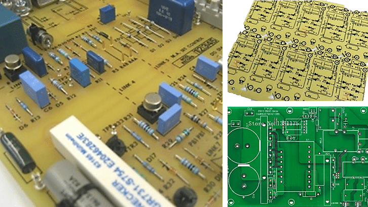
A typical PCB consists of multiple layers, each serving a specific purpose in the overall design. The conductive layers, usually made of copper, are used for routing electrical signals and power between components. The number and arrangement of these layers depend on the complexity of the design and the required functionality. Many of the important performance characteristics of a PCB are defined in the stack-up or the arrangement of layers in the PCB. The layer stack-up is built with alternating layers of conductive and insulating material, and with alternating layers of core and prepreg (two types of dielectrics used in the layer stack-up).
Drop Those Components Like It’s Hot
There are several reasons, but the most common are probably for heat generation or the matching and loading of other circuits with electrical energy. By using a resistor, you can cause the current from one circuit to match that of another, making it easier for electricity to flow between them. The resistance that is generated on an electrical current is measured in ohms, which are derived using a mathematical equation known as Ohm’s Law. Essentially, one ohm is the resistance that is generated when a one-amp current passes through a one-volt resistor, with the current being proportional to the voltage.
Final Rules Check
This process includes etching all of the traces and planes onto the different metal layers and compressing them together, producing a bare board that is ready for assembly. Flexible boards are composed of a less rigid material that allows for far greater deflection. The material is tactilely reminiscent of a film roll, and the board thickness is usually far less than a standard rigid board. While they already see major usage, there is hope that flexible boards will usher in the next step of wearable technology and remove the current planar constraints inherent to rigid board devices. PCBs — which house and interconnect chips, transistors and other components — typically consist of layers of thin glass fiber sheets coated in hard plastic and laminated together with copper.
PCB Layout Design
This includes specialized features that help route intricate traces for high-speed circuits and design rules that can be easily set up for specific area clearances. It also includes having the best simulation tools available to streamline your schematic capture process as well as providing a wealth of library parts to work with. The good news is that there are PCB design tools already available to you that can handle the level of design expertise that we’ve been talking about. Consider the PCB design system from Cadence for all your design tool needs. Plated through-hole technology and its use in multi-layer PCBs were patented by the U.S. firm Hazeltine in 1961.

If you’re planning to have some heat dissipation on your board, do yourself a favor and place extra copper around your surface mount pads. Check out your component datasheets to find all the info you need use your pad surface area as a heatsink. As you can tell by this guide, PCB board design is a complicated thing to perfect. You have to consider spacing, traces, component placement, and many other factors.
Use extra copper
Verify the changes (addition of the SchDoc information to the project without error) by clicking on the Validate Changes tab. If the status for all items is green, then click on the Execute Changes tab. Altium Designer can save you a substantial amount of time during this PCB design step. The white silkscreen layer is applied on top of the soldermask layer.
With these parts ready for use, begin by organizing them on schematic sheets within the CAD tools. Once the parts are roughly placed, wires can be drawn that represents the connectivity between the pins of the schematic symbols. These lines are known as nets, and they can represent single nets or groups of nets for memory or data circuits. During the schematic capture, process parts must be moved as needed to create a schematic that is legible and clear. This manufacturer uses electronic design automation tools to solve complex issues. Soon, the Internet of Things and the 5G market will create more opportunities for this industry.
PCBs Past and Present
Rigid-flex PCBs offer the best of both worlds by combining rigid and flexible substrates into a single board. The rigid sections provide structural support and accommodate components that require stability, while the flexible sections allow for bending and folding in specific areas. This unique combination enables the creation of three-dimensional designs and the integration of multiple circuit boards into a single assembly. Rigid-flex PCBs find applications in space-constrained devices like smartphones, laptops, and medical implants, where reliability and compact packaging are essential.
Electronics Lab to Train Students in Printed Circuit Board Manufacturing - UMass Lowell
Electronics Lab to Train Students in Printed Circuit Board Manufacturing.
Posted: Fri, 02 Feb 2024 08:00:00 GMT [source]
The schematic is a visual representation of the circuit that shows how the components are connected and how they interact with each other. It serves as a blueprint for the PCB layout and is important for ensuring that the final board functions as intended. The schematic consists of various symbols that represent different electronic components such as resistors, capacitors, transistors, and integrated circuits. These symbols are interconnected by lines that indicate the electrical connections between the components.
This is cheaper for each board than photo-resist, but is more expensive in the beginning. Unwanted copper is removed, leaving copper wires that will connect the electronic components. The components are placed on the board, making contact with the wires.
This information is valuable for troubleshooting and fine-tuning the circuit design. Printed Circuit Boards (PCBs) are essential components in modern electronic devices. They provide a platform for connecting and supporting various electronic components, allowing them to function together seamlessly. Creating your own PCB may seem like a difficult task, but with the right tools and knowledge, it can be a rewarding and cost-effective endeavor.
Later, the metal strips were replaced by wires connected to screw terminals, and wooden bases were replaced by metal frames. This let things be smaller, which was needed as circuits became more complex with more parts. In 1925, Charles Ducas of the United States developed a method using electroplating.
The advanced PCB technologies offer unique features and capabilities, enabling the development of more compact, flexible, and high-performance electronic devices. Looking ahead, PCB technology is expected to continue advancing to meet the ever-increasing demands for miniaturization, high-speed performance, and enhanced functionality in electronic devices. Vias are the small holes drilled through the PCB and plated with conductive material, allowing for electrical connections between different board layers.
Conventionally, semi-cured PCB layers are held in cool, dry conditions where they have a limited shelf life before they're laminated in a heat press. Because trimers can form new bonds, researchers laminated fully cured PCB layers. PCBs—which house and interconnect chips, transistors, and other components—typically consist of layers of thin glass fiber sheets coated in hard plastic and laminated together with copper. That plastic can't easily be separated from the glass, so PCBs often pile up in landfills, where their chemicals can seep into the environment. The team tested its vPCB for strength and electrical properties, and found that it performed comparable to the most common PCB material (FR-4).
The most important thing you can do to ensure a smooth PCB manufacturing process and PCB assembly is to follow your manufacturer’s DFM guidelines. Reliance on default or general specifications can cause manufacturing delays and may require design changes. This is easily avoided by setting up your DRCs to match the capabilities of your manufacturer. Forget about learning through trial and error, your PCB design software should guide you through the basic design tools and introduce you to advanced features that maximize productivity. Add to that a vibrant design community, extensive knowledge base, design webinars, blogs written by experts, and an extensive PCB design tutorial, and Altium Designer helps set you on the path to success.
He created an electrical path directly on an insulated surface by printing through a stencil (a shape cut into a board or paper) with special ink that could conduct electricity, just like wires could. A. Proper thermal management is crucial for ensuring the optimal performance and reliability of electronic devices. It helps to dissipate heat generated by components, preventing overheating and potential component failure. Techniques such as using thermal vias, heat sinks, and selecting appropriate PCB materials can help improve thermal management. Multi-layer PCBs consist of three or more conductive layers, separated by insulating material or layers made of prepreg. These boards offer the highest level of complexity and component density, making them ideal for advanced applications such as high-speed digital circuits, RF systems, and aerospace electronics.


No comments:
Post a Comment